#statusMessage#
Do you want to start the comparison now?


Without reliable communication, safe operation is impossible. In the aerospace industry, failures are not an option. At ...

In safety-critical development and manufacturing processes, the test architecture determines quality, cost efficiency, a...

Increasing efficiency requirements in vehicles, data centers, and industry are driving new vehicle electrical system and...
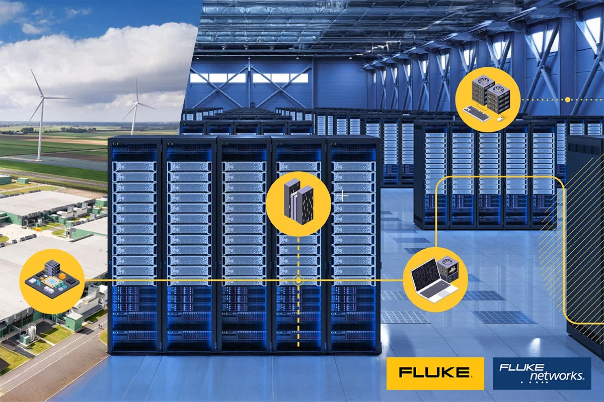
Early prevention, comprehensive certification, targeted troubleshooting. In every area of your data center, measuring in...

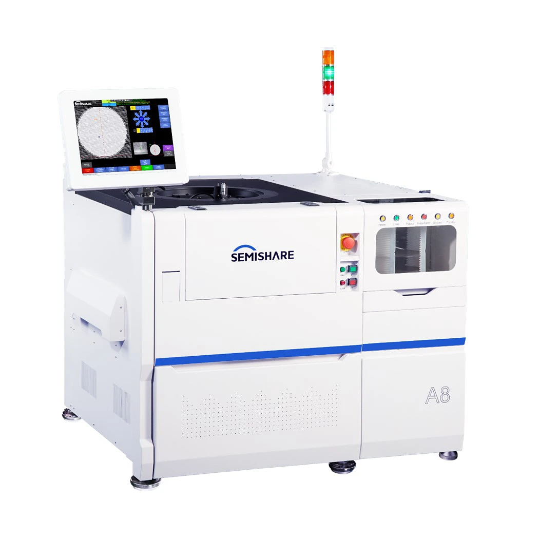
Together with our partner bsw Testsystems & Consulting AG, we advise you on modular wafer probe systems from the manufacturer brands Semishare and Signatone. Each probe station is configured to customer specifications and matched to your individual measurement application with the parameter analyzer.
Would you like to learn more about using your parameter analyzer with a probe station? Please contact our experts.
Gain clarity about the electrical quality of your chips at an early stage and accelerate product development. If process deviations are detected quickly, scrap or rework can be avoided and failure costs reduced.
Electrical measurements with a wafer probe station are performed using suitable measuring instruments. Parameter analyzers and curve tracers provide special integrated functions required for systematic semiconductor characterization. The parameter analyzer combines measurement functions such as IV, CV or pulse measurements as well as synchronized SMU channels in one system. The curve tracer focuses more strongly on displaying and evaluating IV characteristics. Both measuring instruments are used to visualize the behavior of components such as diodes, transistors or SiC/GaN power semiconductors.
As a BSW partner, we can provide you with a complete test solution for wafer characterization using probe stations. Together with a parameter analyzer or curve tracer from Keithley, Iwatsu and Keysight, you receive a highly efficient system for precisely contacting and measuring your device under test.
The combination of probe station and parameter analyzer provides you with a complete solution for semiconductor characterization at wafer level.
Application Engineer

| Applications | Examples |
|---|---|
| Wafer and component characterization | WAT/CP test, DC/IV/CV characterization, tests on wafer diodes and transistors |
| Reliability and stress testing | Aging and WLR test, high-voltage/high-current test |
| RF/mmW test | 1/f noise test |
| MEMS and optoelectronics test/b> | LD/LED/PD test (intensity and wavelength) |
| Material/failure analysis | Evaluation of defects and process deviations |
| Special measurements | Low-current test down to 100 fA |
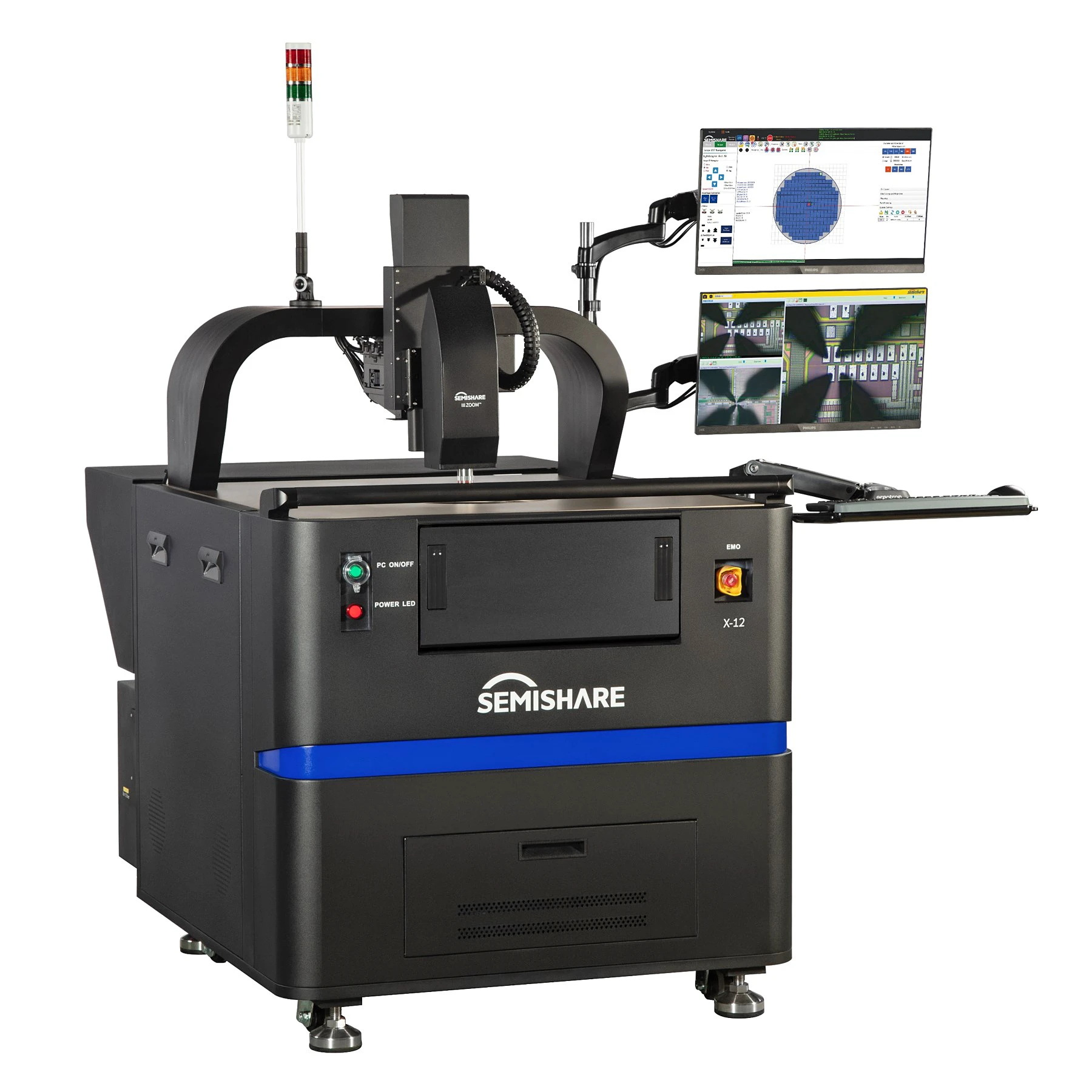
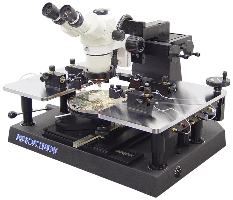
The probe stations from Semishare and Signatone support precise on-wafer measurements from manual analysis to fully automated test sequences with high throughput. Depending on the model variant, the systems offer high positioning accuracy, stable chuck and motion platforms, and innovative imaging functions. Measuring instruments such as your parameter analyzer or curve tracer can be easily integrated. This enables a wide range of measurement tasks in research, development and production-related quality assurance to be implemented efficiently.
1. The wafer is placed on the chuck of the probe station.
2. The wafer is aligned using the microscope, camera and positioning system.
3. The probes are lowered onto the device under test. Stable contact force with low contact resistance and reproducible positioning are decisive.
4. The parameter analyzer is connected to the probes via measurement cables.
5. The analyzer applies defined voltages and currents, measures the electrical response of the device under test and generates IV/CV characteristics.
6. In semi-automatic or fully automatic systems, the probe station automatically moves to the next test structure. The measured values are stored for wafer evaluation.
7. The data show, among other things, process deviations, defective dies, edge-zone effects, outliers or systematic manufacturing problems.
Would you like to learn more about wafer probe stations for your application?
As a partner of BSW, we are available for a consultation.
SEMISHARE is a leading manufacturer of modular wafer probe systems for individual test requirements in the semiconductor industry. Its main applications include WAT/CP tests (wafer and circuit tests), RF/mmW tests, I-V/C-V tests, and MEMS and optoelectronic component tests. Headquartered in China, the company has an international orientation and works with distributors such as BSW.
Signatone is a US-based manufacturer of manual and semi-automatic wafer probe systems for flexible test applications in the semiconductor industry. Typical application areas include on-wafer probing, component characterization, and material and failure analysis. Headquartered in California, the company has an international orientation and works with distributors such as BSW.
.webp "Seminar LabVIEW Core 1")