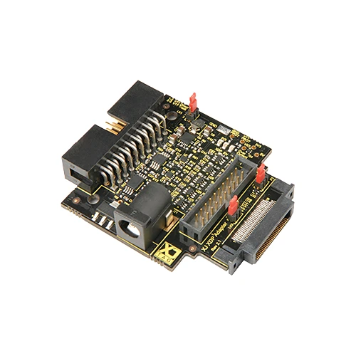
The XDP-0010 from XJTAG is a high-performance low-voltage boundary-scan adapter for connecting an XJLink2 controller to a device under test. It converts JTAG signals from the XJLink2’s 3.3-V voltage range to the lower signal voltage of the device under test. The target voltage is regulated via a VTT reference provided by the device under test and can range from 0.6 V to 3.2 V during normal operation.
Thanks to its particularly low-impedance output drivers, the adapter is also suitable for JTAG interfaces with terminating resistors as low as 25 Ω. This enables reliable signal transmission at high clock rates and under demanding electrical loads. The moderated rise and fall times reduce overshoot and support high signal integrity.
The XDP-0010 is installed between the XJLink2 and the device under test. For connection to the device under test, both an Intel XDP-compatible connector for direct mounting on the target board and a 20-pin connector with a 2-mm pitch are available for flexible cable connections. Direct mounting via the XDP connector minimizes cable lengths and is particularly suitable for applications with high TCK frequencies.
Typical applications include boundary-scan testing, commissioning and troubleshooting on electronic assemblies, production testing, and the analysis of processor and embedded systems with low JTAG signal voltages. An integrated overcurrent shutdown protects the output drivers in the event of short circuits or excessive load. LEDs indicate the operating status, the activation of the output drivers, and a possible overcurrent shutdown. Power is normally supplied directly via the XJLink2; if higher power is required, an external power supply can also be connected.
Product Features:
- Dimensions including connectors: 56 × 47 × 15 mm
- Maximum TCK frequency: up to 100 MHz, depending on cabling and impedance
- Signal voltage at the XJLink2: 3.3 V
- JTAG voltage range with VTT tracking: 0.6 to 3.2 V
- JTAG voltage range with direct external VTT supply: 0.3 to 3.3 V
- Supported signals: eight level-shifted signals, including five downlink and three uplink signals
- Output impedance: less than 2 Ω at 1 V
- Supported termination resistances: down to 25 Ω
- Rise and fall times: approx. 1 ns without load, 2 ns at 50 Ω, and 3 ns at 25 Ω
- Maximum combined output source current: 250 mA before protection shutdown is triggered
- Maximum combined output sink current: 250 mA before protection shutdown is triggered
- Quiescent current consumption: 20 mA
- VTT reference load: 10 kΩ to ground
- Input threshold: VTT/2
- Input hysteresis: 50 mV
- Input current: less than 2 µA
- External supply voltage: 5 to 15 V
- XJLink2 connector: 20-pin, dual-row, 2.54 mm pitch
- Alternative target connector: 20-pin, dual-row, 2 mm pitch
- Intel XDP connector: Samtec BTH-030-01-L-D-EM2
- Protection features: Overcurrent shutdown and ESD protection
- Status indicators: LEDs for power supply, output enable, and overcurrent